About Minimal Fab and the ICPS PDK
Introduction
Recently I participated in the Minimal Fab Design Contest. I had a go at designing a transmission-gate D-FF using the provided template for the layout. You could only use the first metal layer to connect devices.
It was actually selected for fabrication! This image shows the layout of the wafer with all the submitted designs:
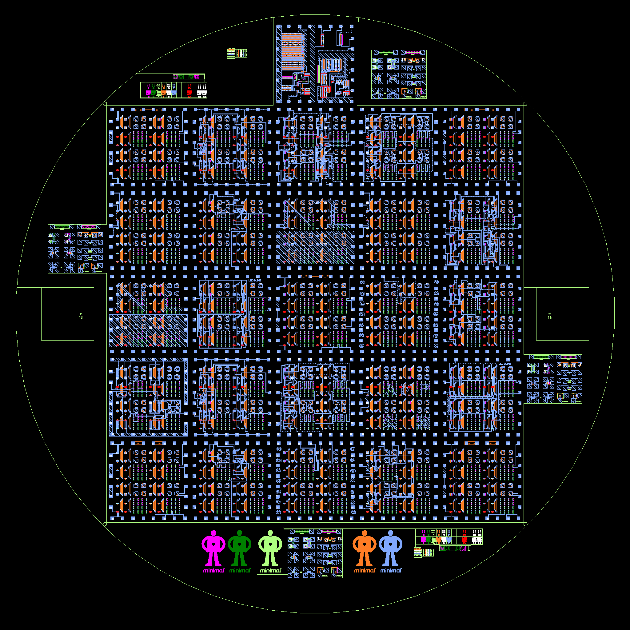
My design is the second die in the first row of the 5x5 array.
This was only possible because the Industrial CPS Research Center (ICPS) at AIST (Advanced Industrial Science and Technology) in Japan open sourced their PDK for the Minimal Fab SOI-CMOS process. In a follow-up blog post I would like to show you, how you can create your own design for this process.
This blog post is about Minimal Fab and the ICPS PDK.
Minimal Fab and the ICPS PDK
The ICPS Process Design Kit (PDK) is used to design chips for the Minimal Fab system.
The ICPS PDK contains the following data:
- Documentation
- Device/Process Explanation
- Device Characteristics
- Design Manual
- Electrical Data
- SPICE Model
- PCELL
- DRC/LVS Rule
The following devices can be realized
- TiN-gate PMOS and NMOS devices
- p+ diffusion resistance
- n+ diffusion resistance
- TiN capacitance
- Diffusion capacitance
The process can withstand a voltage of up to 7V.
The minimum gate length of the process is 6um, which would date it to the early to mid 1970s. The first commercially available microprocessor, the Intel 4004, was designed using a 10 um process to put things in perspective. But the Minimal Fab is a new development, so why bother creating something that can't produce state-of-the-art chips?
The answer to that is the way how a Minimal Fab works and what its intended use is. Compared to a Megafab, which costs billions and produces chips with feature sizes in the nm range, a Minimal Fab only costs in the range of tens of millions, doesn't require a clean-room and can produce prototypes in as little as 10 days.
How is this possible? Well, first of all, the wafers are transported in so called shuttles, which act as a portable clean-room for each wafer, also blocking UV radiation. Because production is on an individual wafer basis, it is possible to get rapid feedback on your design.
The wafers are therefore small: half-inch wafers or, for the rest of the world, 1.27cm in diameter.
The system is built in such a way that each process step can be done by a machine of standard size: 11.8in by 17.7in, with a height of 56.6in or approximately 30cm by 45cm and 144cm height.
The most important part: there are no masks used in the process.
The features are applied through direct drawing exposure. This saves money and time, but also reduces the minimum feature size to approximately 5um.
As you can see, the target audience is a completely different one. While a Megafab produces chips that may end up in your phone, a Minimal Fab is mainly for research and development, so-called High Mix Low Volume (HMLV) manufacturing cases.
I can recommend this video for an overview of the production process: Semiconductor Manufacturing Process for Minimal Fab
What's SOI-CMOS?
Okay, now we know what a Minimal Fab is and what the PDK is used for. But what does SOI-CMOS mean?
The majority of all chips nowadays are fabricated using CMOS technology. One of the big advantages of CMOS is that there is almost no static power consumption (ignoring leakage) thanks to symmetrical pairs of p-type and n-type MOSFETs.
In addition, the process also uses SOI - Silicon On Insulator technology.
With SOI, each device is electrically isolated from each other, there is no common substrate and therefore no need for a bulk connection. SOI has a lot of benefits over conventional CMOS, namely lower parasitic capacitance, resistance to latchup, higher density and overall higher performance.
So don't you dare comparing this process with a mid-1970s one ;)
When designing circuits, this also means we can simplify things:
Our PMOS and NMOS transistors only have three connections that we need to care about instead of four: Gate, Drain and Source, with Drain and Source being interchangeable.
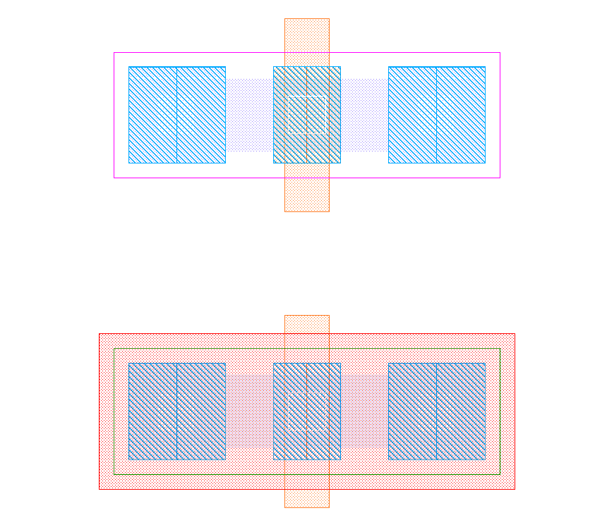
PMOS at the top and NMOS at the bottom. Both transistors are minimum size with a Length of 6um and a Width of 10um.
Conclusion
At this point you should have a rough idea of what a Minimal Fab is and how it is used to produce integrated circuits quickly and cost-effectively. Also you know that a Process Design Kit contains all the data necessary to design a circuit for a certain process and that the ICPS PDK is just that for the Minimal Fab.
So what is missing? Actually designing a circuit :D I'm currently in the middle of writing a step-by-step tutorial on how to use the ICPS PDK to design a simple NAND gate that could be fabricated using the Minimal Fab system.
Stay tuned!