Design of a NAND gate using the ICPS PDK
Table of Contents
Introduction
In this blog post I would like to show you how to create your own NAND gate using the newly released ICPS PDK. I highly recommend following the tutorial for yourself to get some hands-on experience. For comparison, you can find all the resulting source files in this repository.
If you have no idea what a Minimal Fab or the ICPS PDK or SOI-CMOS is, fear not! Please read my previous blog post which elaborates on exactly these points.
Let's get started!
Tools Setup
Luckily, the PDK is not only open source, but it is also designed for open source tools. We will be using xschem for schematic entry, ngspice for simulation purposes and KLayout for the layout of the design.
The tutorial was designed for and tested under Linux. It should also work on Windows and Mac OS, but it's hard to test for something you don't use ;)
Whatever you do, please make sure to install recent versions of the tools. If you are using Linux, depending on your distribution the packaged tools can be quite dated.
For Windows and Mac OS I would recommend to get the KLayout binaries directly from the website. On Linux I installed KLayout via Flatpak, which works great.
There seem to be up-to-date Windows binaries for xschem here. On Mac OS and Linux it seems you need to compile xschem yourself.
For Linux and Windows, ngspice provides binaries at the download page. You can get ngspice on Mac OS via Homebrew.
For me, the approach was to compile xschem and ngspice from source and install Klayout via Flatpak.
Next, you will need to install the ICPS PDK.
PDK Installation
KLayout allows the installation of packages via it's "Salt" package manager. For now, the ICPS PDK is not yet available via the "Salt.Mine" package index service. This means we have to install it manually into the correct directory.
We will install two packages that will allow us to select the ICPS2023_5 technology in KLayout.
What about xschem and ngspice? These packages also contain the schematic symbols and simulation models. So we will point xschem and ngspice to the correct directories later on.
Linux
On Linux you just need to clone these two repositories:
under ~/.klayout/salt/. That's it!
cd ~/.klayout/salt/
git clone https://github.com/mineda-support/AnagixLoader.git
git clone https://github.com/mineda-support/ICPS2023_5.git
If the salt/ directory does not yet exist, create it.
Windows and Mac OS
The installation procedure should be the same as under Linux. You can also download the packages from GitHub and extract them manually. The path to the salt/ folder under Windows is c:\users\you\KLayout\salt, were you is your username.
If you start KLayout now, you should see the option to select the ICPS2023_5 PDK. This means that the installation of the PDK was successful.
Under the menu item Macros you will now find a number of additional entries.
Drawing the Schematic
The first step in our journey is to draw the schematic.
Before we start xschem, we need to configure the xschemrc file. Therefore, create the file xschemrc under ~/.xschem if it does not exist yet. Set the content of the file to:
append XSCHEM_LIBRARY_PATH :$env(HOME)/.klayout/salt/ICPS2023_5/Technology/tech/symbols/Xschem
set terminal gnome-terminal
For Windows and Mac OS, adjust the path accordingly and omit set terminal gnome-terminal.
The first line tells xschem where it can find the symbol libraries.
The second line tells xschem which terminal emulator to use. Xschem will use gnome-terminal instead of the default xterm to start the simulation via ngspice.
Enough of the preparations, let's create the schematic!
We are going to design a NAND gate. Create a new directory for your design and start xschem from the command line as follows:
xschem nand.sch
You should now see a black, blank canvas.
Press the Insert key. In the window that opens, navigate to ~/.klayout/salt/ICPS2023_5/Technology/tech/symbols/Xschem. This is the ICPS symbol library. On the right side you can select various symbols. We want to add a NMOS_MIN and a PMOS_MIN. In total we need two PMOS and two NMOS transistors. You can copy symbols by selecting them and pressing c.
Now edit the transistors by selecting them and pressing q. Delete all properties after the name. For the PMOS we want to use l=10.0U w=40.0U and for the NMOS l=10.0U w=10.0U. These are the same values as in the Minimal Fab design contest template. Of course you could set other values for L and W, with a minimum of 6u for L and 10u for W.
Next, press the Insert key again and navigate to the ICPS symbol library. Here we need ipin for the inputs opin for the output and iopin for the power supply. Change the names to VDD, VSS, A, B and Z. Use shift + f to flip symbols.
You can move symbols by selecting them and pressing m. Use w to draw wires and connect all symbols accordingly.
Finally, your schematic should look somewhat like this:
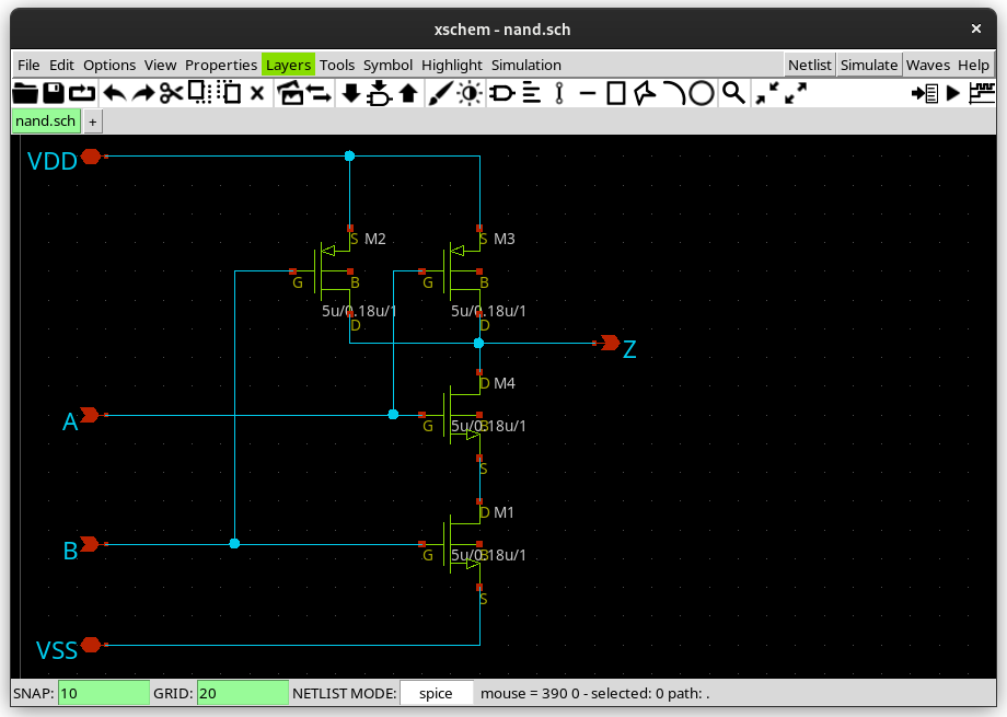
Note that we do not connect the bulk connection of the transistors because we use SOI technology.
Before we go on, press a to automatically create a symbol for your circuit (nand.sym). We will need it later.
Create the Netlist
To create the netlist for your circuit, press the Netlist button on the right side of the menu.
By default, the nand.spice netlist is created under ~/.xschem/simulations/. You can change the location where the netlist is saved under the menu item Simulation -> Set netlist Dir. We will need the netlist later for LVS.
You should get a window with some messages Error: undriven node: XXX, which you can ignore since our circuit will be instantiated in a testbench.
The individual wires of your circuit should now be colored like this:

Simulation
We want to run a transient simulation (over time) to make sure our circuit behaves as intended. To do this, we need a testbench that supplies the signals to our NAND circuit.
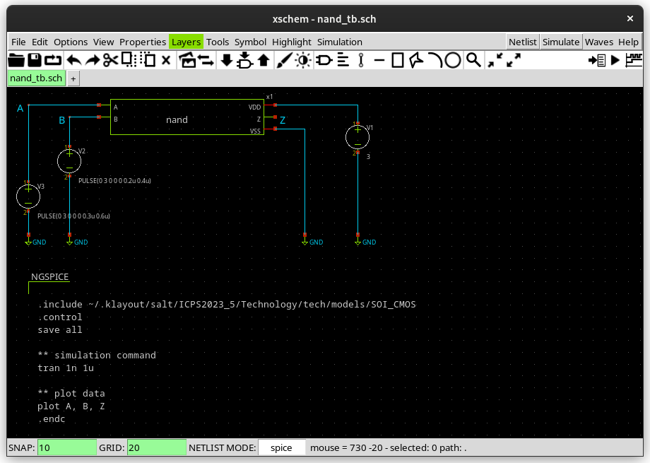
Create a new schematic: xschem nand_tb.sch
Press Insert and then click on Current dir. Now select nand.sym, the symbol that we created earlier.
Additionally, place voltage, vpulse, gnd and code_shown from the ICPS symbol library.
The value of the two vpulse sources should be set to
value="PULSE(0 3 0 0 0 0.3u 0.6u)"value="PULSE(0 3 0 0 0 0.2u 0.4u)"
In this way, we get all possible input combinations for our NAND gate.
The value of the voltage source can be kept at 3 Volts.
For the code_shown symbol, edit the properties and set them to:
name=NGSPICE only_toplevel=true value="
.include ~/.klayout/salt/ICPS2023_5/Technology/tech/models/SOI_CMOS
.control
save all

** simulation command
tran 1n 1u

** plot data
plot A, B, Z
.endc
"
These are the simulation directives for ngspice. They tell ngspice where to find the models, for how long to simulate and which signals should be plotted.
Next, connect everything up, like so:
After clicking on Netlist and Simulate in the menu, you should get the following waveforms:
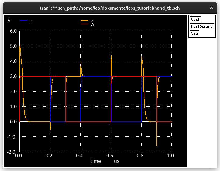
Congratulations! If you see the same result, you have done everything right (and the tutorial works).
We can see that only if both inputs are high, the output is low - the functionality of a NAND gate.
It can be somewhat difficult to see the individual signals in one plot. If you would like to have one plot for each signal, change the plot directives like so:
plot A
plot B
plot Z
If you want proper waveform viewing, take a look at xschem-gaw.
Drawing the Layout
Now that we have completed the first half of this tutorial, we can move on to draw the layout for our NAND gate.
Open KLayout in editor mode. On Linux this is done by passing the -e flag. For example with klayout -e or in my case via Flatpak flatpak run de.klayout.KLayout -e. Under Windows there should be an extra start menu entry.
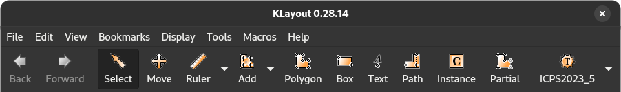
You will see that you now have more options and buttons in the menu.
Go to File->New Layout, select ICPS2023_5 and leave everything as default.
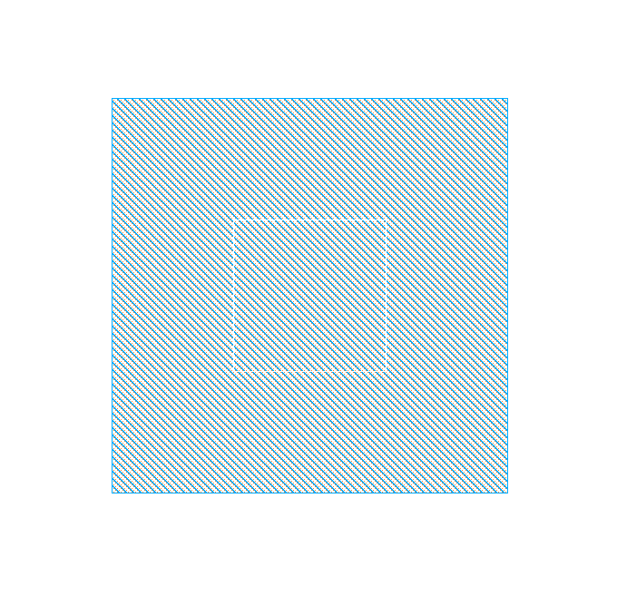
Let's draw a transistor!
Click on Instance at the top. On the left side you will see new options. Under the Instance tab select the library PCells_ICPS2023_5 - PCells and under Cell select Pch for a p-channel mosfet.
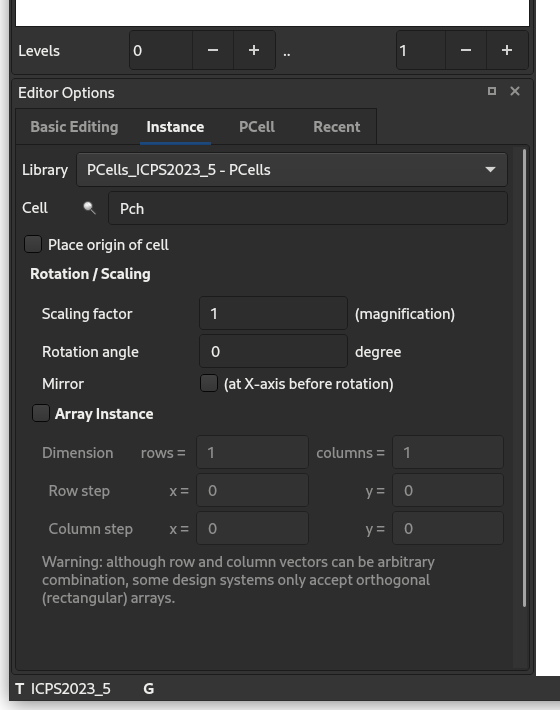
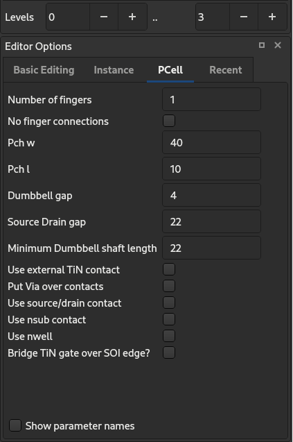
On the next tab, PCell, we can configure our parameterized cell: width and left should already be at 40 and 10. Remove all the check marks that are enabled. We really just want a basic transistor.
Next, place the cell in the empty window by clicking anywhere in it. Initially, you will only see a rectangle with the name of the cell. To see the actual layout, select TOP in the cell browser and select Show As New Top. If that did not help, also select Show All.
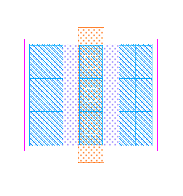
And there we have it! A p-channel mosfet of width 40u and length 10u. The three metal wires connect to drain/source, which are interchangeable, and the gate in the middle.
Let's create another p-channel mosfet with the same size and two n-channel mosfets with w/l = 10/10. Again, uncheck all check marks.
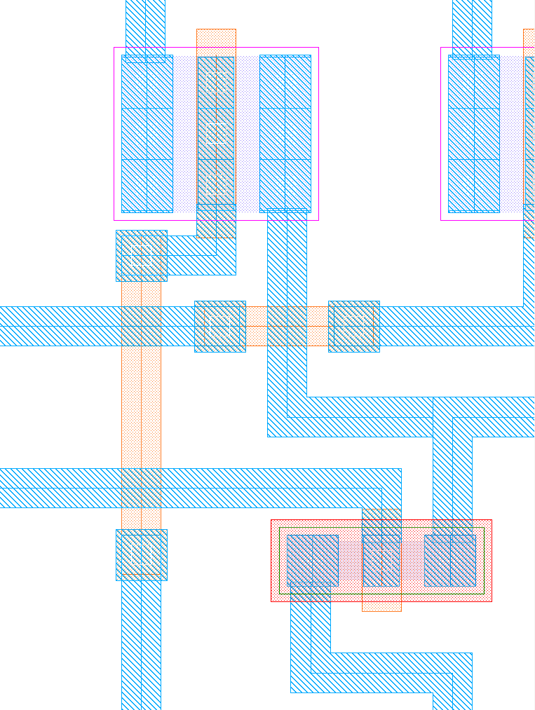
Next, select the ICPS2023_5_Basic library and place 5 instances of the cell PAD60.
It should look somewhat like this:
Select the ML1 layer on the right side and click on Path at the top. We will use the metal layer to connect the transistors with each other and the pads. Make sure there are no gaps between metal paths that should be connected. You can also overlap paths just to be sure.
The result should look like this:
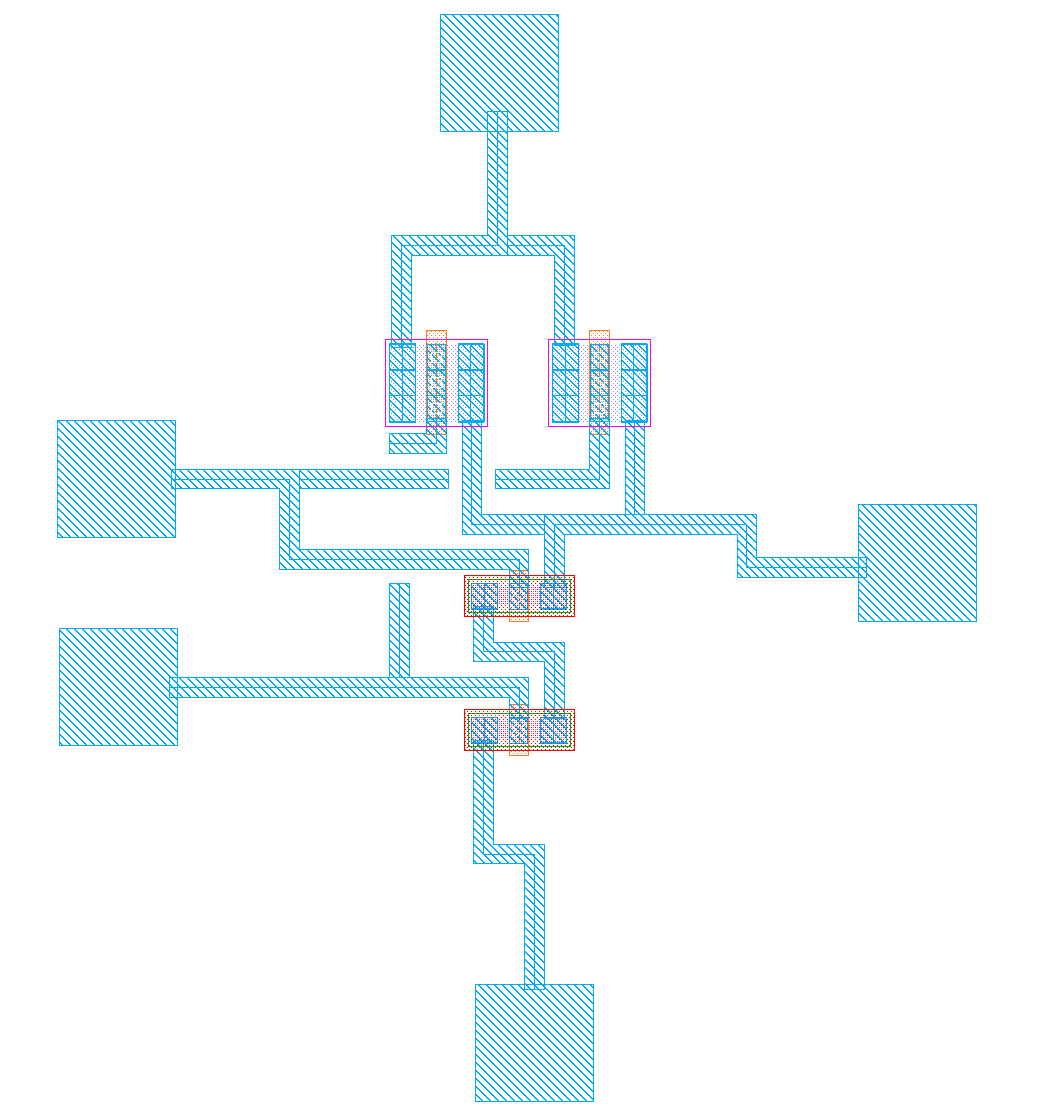
But we have one problem! We can't connect the gates of the p-channel mosfets without going around the pads. The solution is to use the TIN layer to go underneath ML1. It is basically a bridge underneath the metal layer.
To get a contact between ML1 and TIN1 we need to place a pcont cell. You can fint his cell in the ICPS2023_5_Basic library.
Basically, the pcont cell consists of a metal layer and an underlying TiN layer with a contact in between. So why don't we just draw them ourselves? Well, connections and vias often have strict requirements. For connections in the CNT layer the size has to be 5x5um. By using this cell, we ensure that there won't be an issue.
Here you can see how I placed the pcont cells:
Now, just add some labels to the pads by selecting the TEXT layer and clicking on the Text button. I had to set the TEXT layer to black to be able to see the text on the white background.
And the layout is complete!
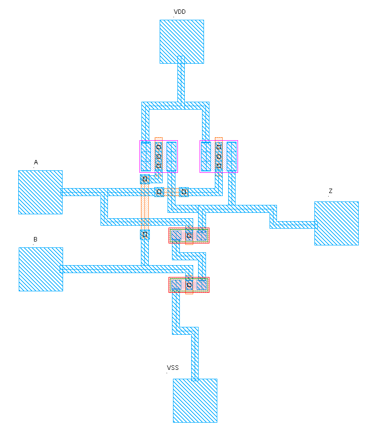
I am sure you can do this much more area efficient ;)
Performing Checks
Manufacturing a chip is costly, and so you want to be pretty sure your design is correct before sending the layout to the fab.
We will make use of two checks to increase our confidence in this regard.
DRC - Design Rule Check
The first is the DRC - Design Rule Check. With this check, we make sure our design is actually manufacturable. For example, no metal path is too thin, or the distance between two paths too narrow. Therefore DRC analyzes your layout based on the DRC rules from the PDK and prints the results.
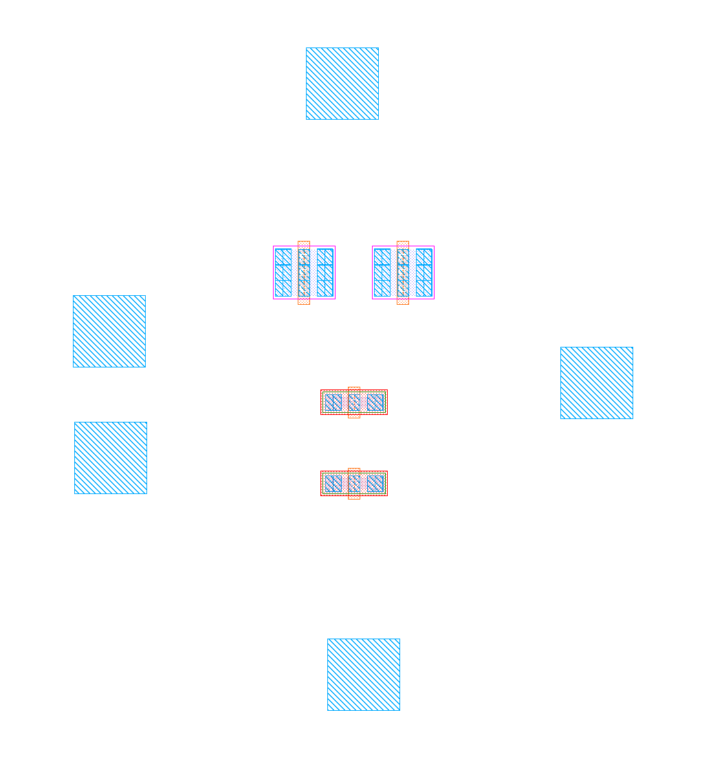
In KLayout, when your layout is loaded, select Tools->DRC->DRC for ICPS2023_5. This will open the Marker Database Browser. By clicking on the green play button we start the DRC.
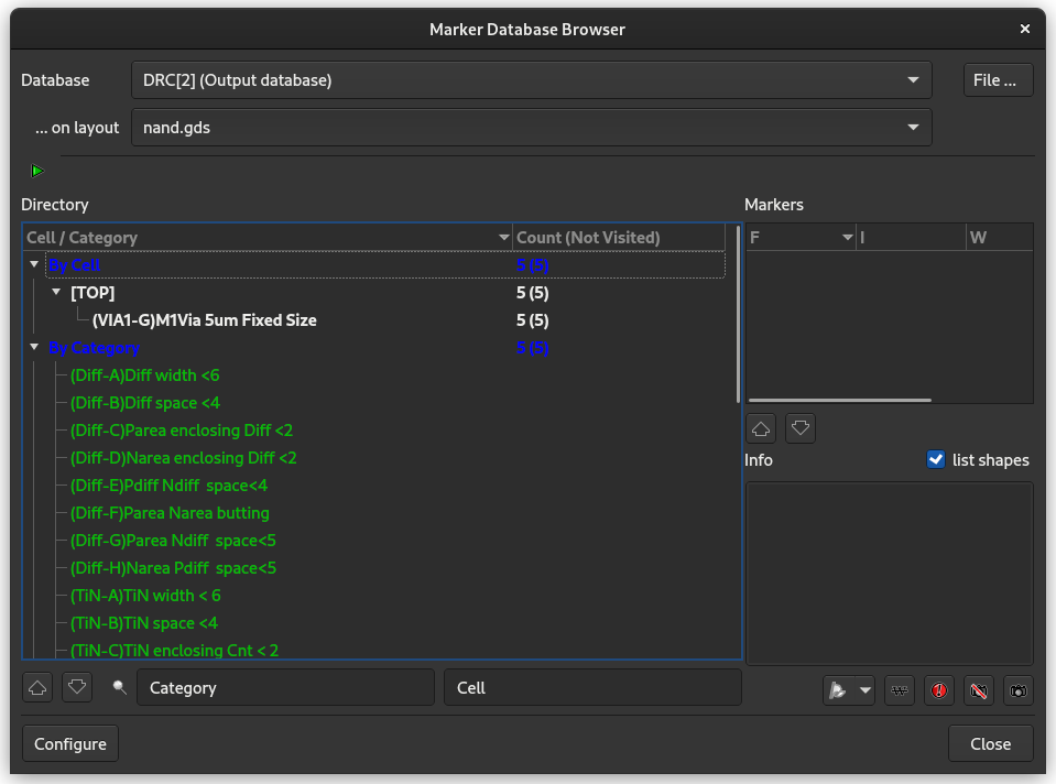
And indeed there is one problem!
It refers to the VIA1 layer and says that only vias of a fixed size of 5x5um are allowed. But we did not even use VIA1, right? Yes, but the PAD60 contains a VIA1 larger than 5x5um and that's where the error comes from.
In this case we ignore the problem and this will probably be fixed in a future PDK update. We don't even know if the PAD60 is ready to be used ^^
DRC Troubleshooting
Another example for a DRC error would be (ML1-B)Ml1 space < 4. This happens when the spacing between ML1 is too narrow.
If you click on the error, KLayout will show you the issue in the layout:
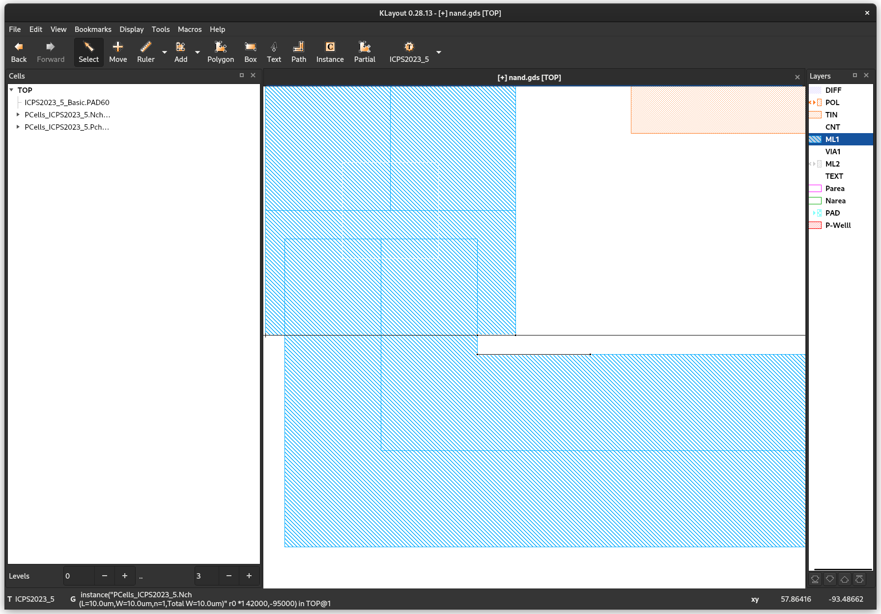
In this case the gap between ML1 is too narrow and could lead to problems during manufacturing. The solution would be to remove the gap, either by increasing the width of the smaller path or by moving it.
If you have other DRC issues, try to understand them and fix them in your layout before continuing with LVS.
LVS - Layout Versus Schematic
Next, we use the LVS - Layout Versus Schematic check to make sure the layout is actually equivalent to our circuit. For example, in an extreme case our layout could just be empty. Then DRC would still pass, but it would certainly not represent our intended circuit.
Therefore, during LVS, a netlist is built from just the layout - what devices are present and how are they connected to each other - and this netlist is compared to the spice netlist of our NAND gate. If they match, LVS passes.
LVS checks that the transistors are connected correctly to each other and that their dimensions (W/L) are the same as in our NAND circuit.
First we need to select the netlist created by xschem. To do this, select Macros->Get reference for ICPS2023_5 in KLayout. By default, xschem will store the spice netlists under ~/.xschem/simulations/. Select nand.spice.
In KLayout select Tools->LVS->LVS for ICPS2023_5. The Netlist Database Browser opens and displays the result of LVS.
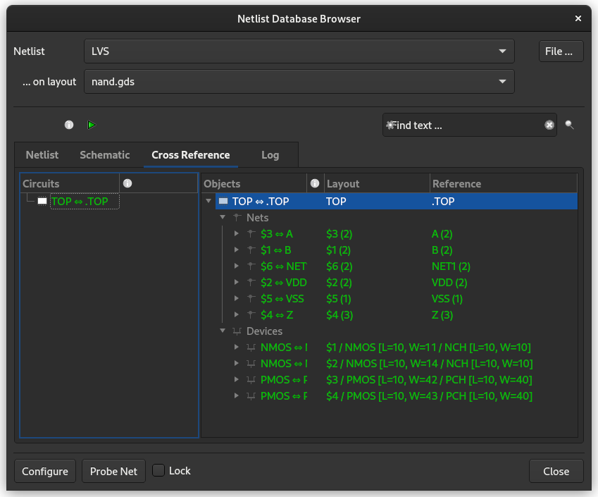
Congratulations! If everything is green, it means the layout is equivalent to our NAND circuit and we could continue with fabrication.
LVS Troubleshooting
If your LVS results show errors, don't despair, but check your layout and schematic again:
- Are there the same number of NMOS and PMOS transistors?
- Are the dimensions of the transistors the same? (W/L)
- Are the transistors correctly connected to each other?
- Is there a
CNTvia betweenTINandML1where they should be connected?
Final Words
Now that you have successfully completed this tutorial, how about tackling a different design? For example an XNOR gate? A D-FF? An amplifier? You can use not only transistors, but also resistors and capacitors from the cell library.
I am excited to see what you will make!