iCEBerg-FPGA
Introduction
Now that I am immersed in the world of digital design, I wanted to create my own FPGA development board. There are two boards that I really like: the iCEBreaker and the ULX3S.
The ULX3S uses an FPGA from Lattice's ECP5 series, which offers a lot of resources.
The iCEBreaker is based on Lattice's iCE40 series, a much less powerful FPGA with fewer resources but also lower power consumption.
I decided to replicate the iCEBreaker, but in my own way. There is also the iCEBreaker-Bitsy, which is not released at the moment, but whose files are available. It has a much smaller form factor, and instead of using an FTDI chip, it uses the FPGA itself to communicate via USB.
This is a really clever use of resources, and so I came up with a plan: an FPGA devboard with proper PMOD headers, but USB communication via the FPGA - simple enough.
The result:
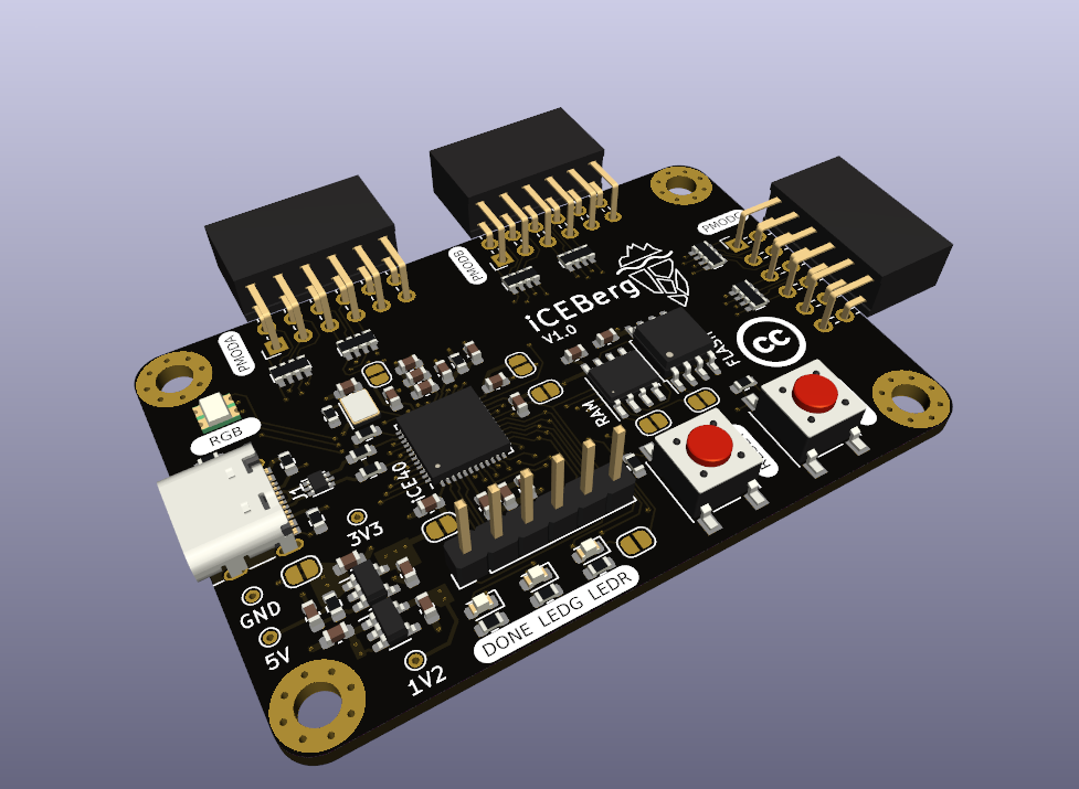
Here you can find the repository for the iCEBerg FPGA development board.
In addition to the FPGA, the board has the following features:
- USB-C connector
- 3 PMOD connectors (A, B and C)
- 12 MHz oscillator
- RGB LED
- LEDs
- DONE (FPGA configuration is done)
- LEDG (user controlled)
- LEDR (user controlled, must be connected first)
- SRAM
- 64Mbit
- Quad SPI
- FLASH
- 128Mbit
- Quad SPI
- To store bitstream and user firmware.
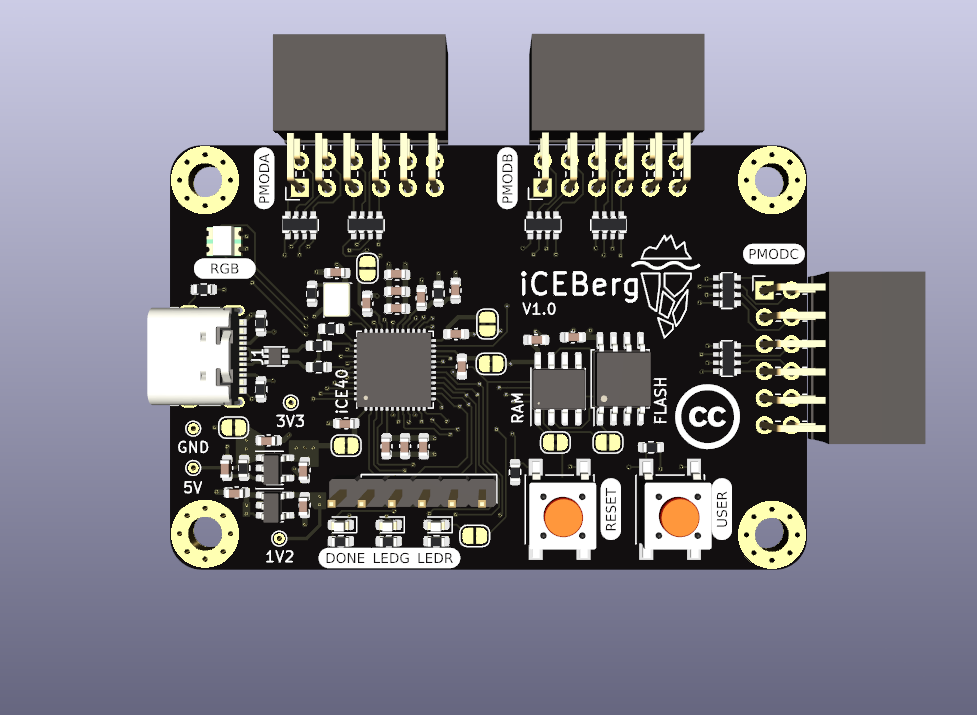
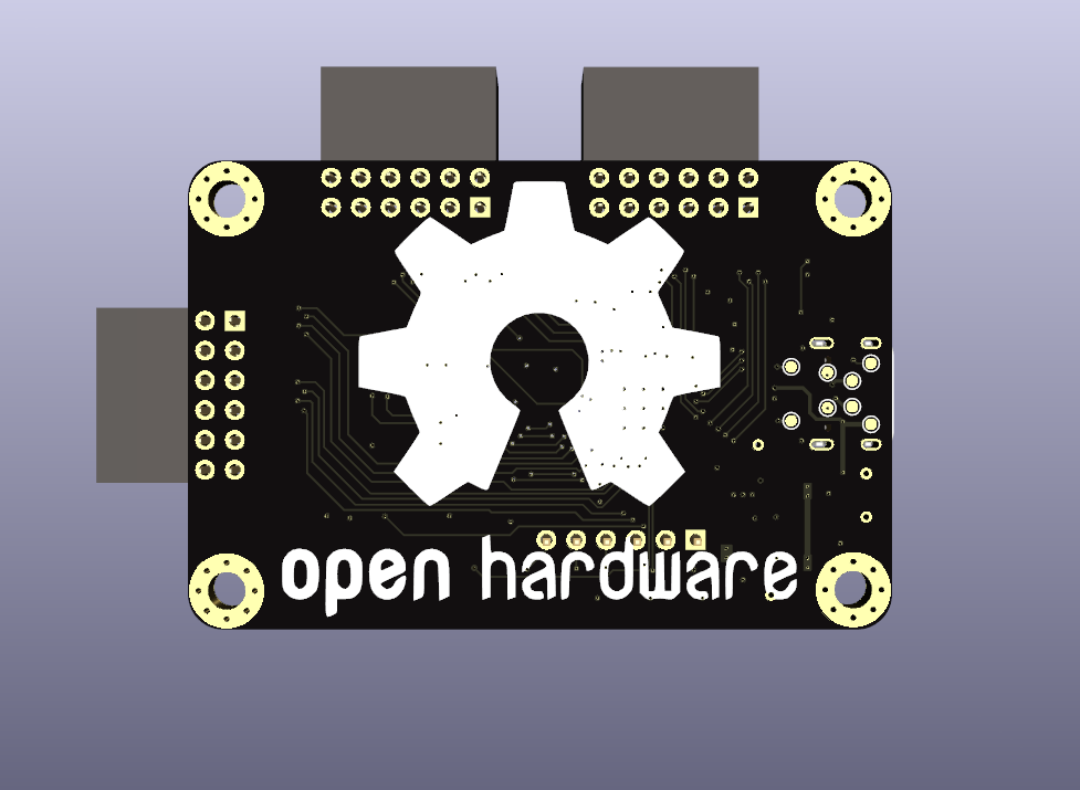
Here are some other views:
 |
 |
Schematic
The schematic is mostly a 1:1 copy of parts of the iCEBreaker and the iCEBreaker-Bitsy. I am very grateful that the schematics are available as open source.
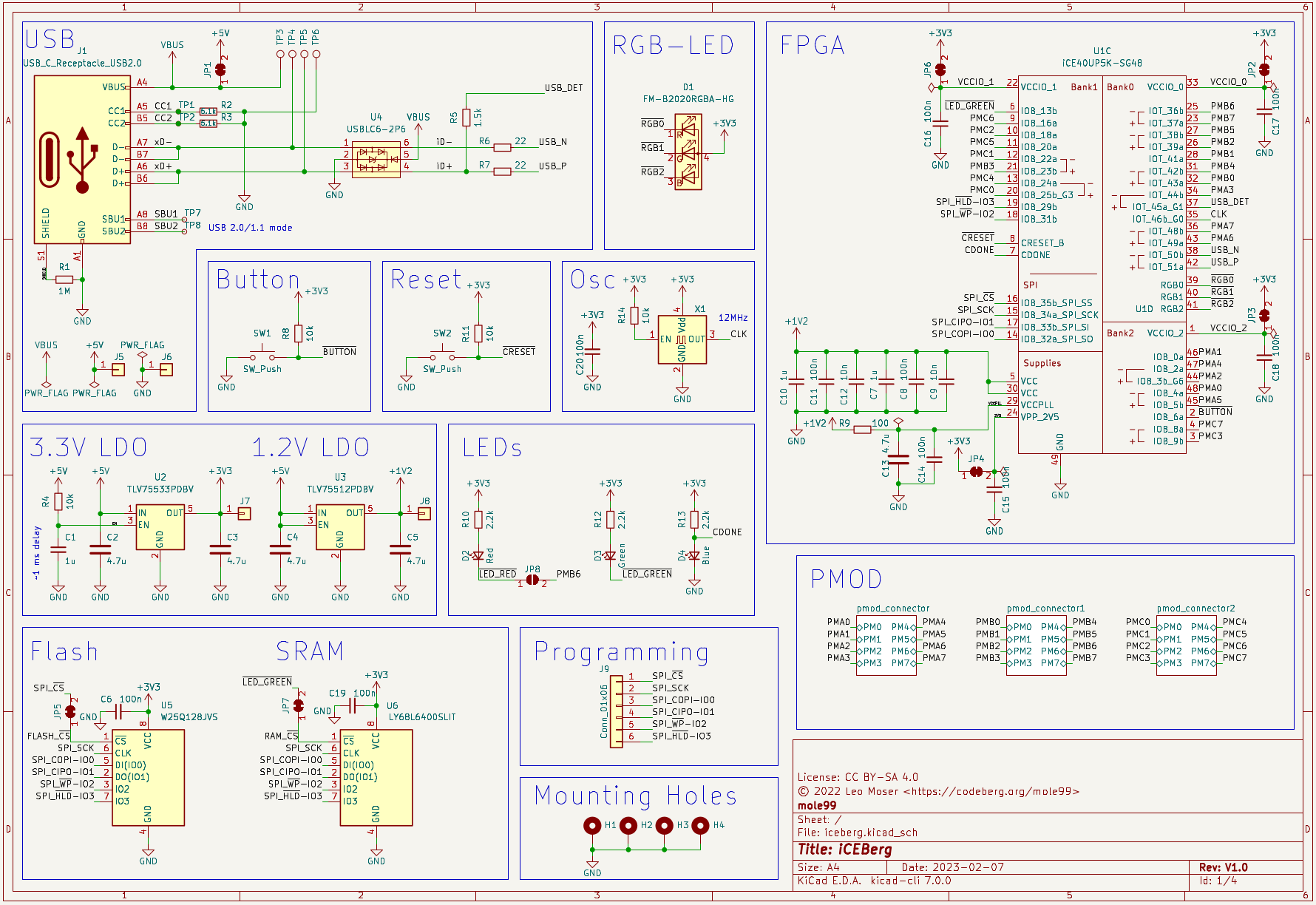
I created my own symbol for the iCE40UP5k: the three banks and the supply are separate and can be moved to different sheets. In this case, I placed them all together.
Board View
This is the top view of the board:
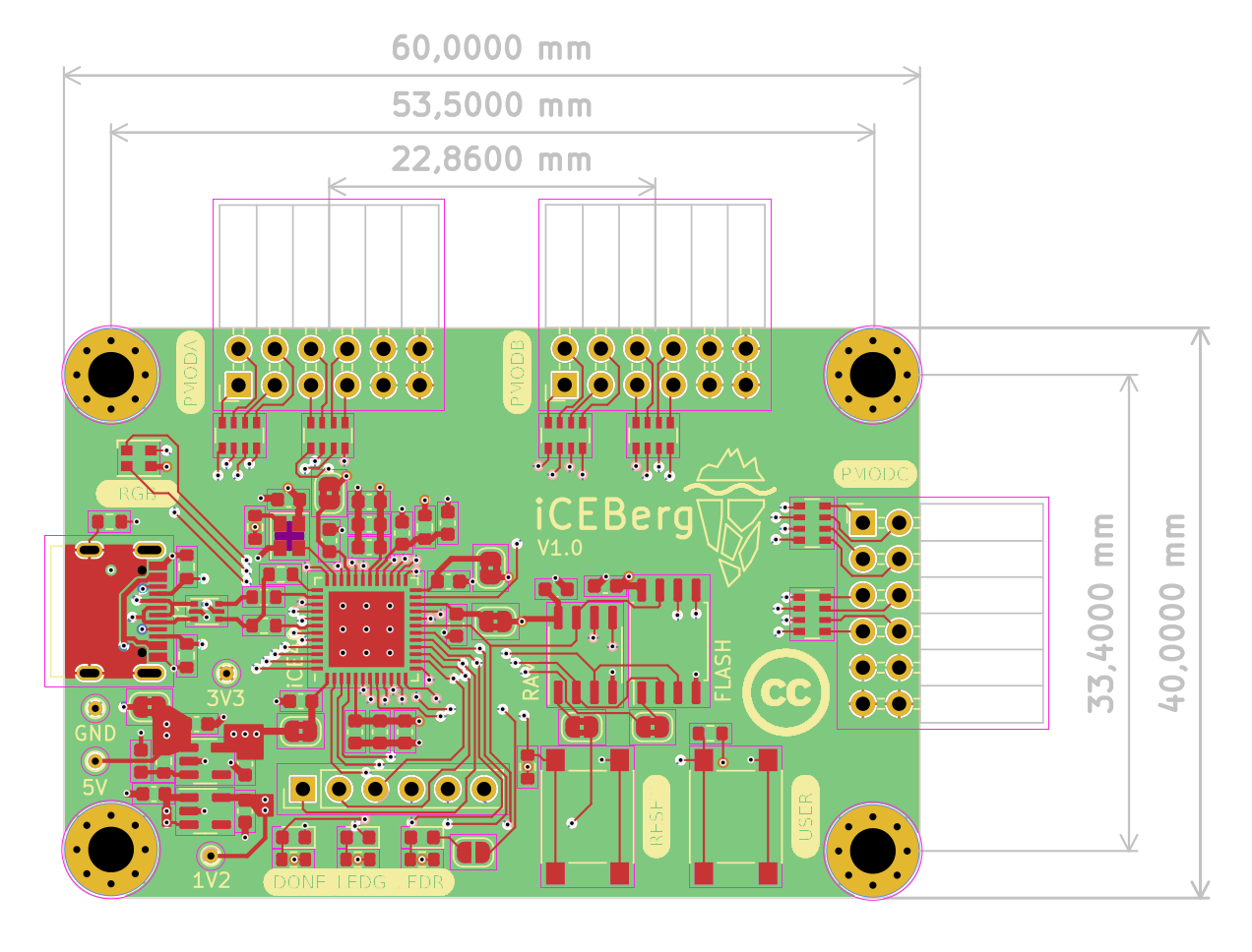
As you can hopefully see, I tried to make it look pretty. With a custom logo and silkscreen labels created in Inkscape.
Manufacturing
To save time on manufacturing, I decided to use JLCPCB's SMT service. Almost all parts are assembled by them, except for the iCE40UP5k and the FLASH chip, since I already had them at home :)
This also allows me to preload the FLASH with the bitstream of the bootloader before soldering. You will hear more on that once I receive the boards and do the bring-up.
Summary
Although it is not the most original board, it was a good exercise to build it. I learned a lot and became even more confident in designing PCBs.
Who knows, maybe next time I'll try a more daring design ;)